PCB Designing

Course Description

PCB Designing

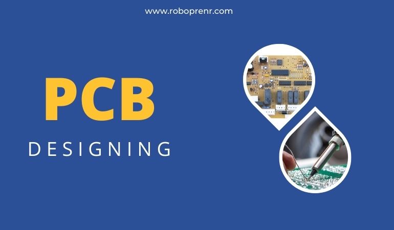
What is PCB design? Printed circuit board (PCB) design brings your electronic circuits to life in the physical form. Using layout software, the PCB design process combines component placement and routing to define electrical connectivity on a manufactured circuit board.

Course includes a take away PCB design kit with all the required devices and components to solder, etch and produce your own permanent circuit boards.

    • Session 1: Introduction to PCB

      Concepts - Components, Pads, Vias, Traces, Silkscreen, Soldermask, Soldering Tools and apparatus 

      Hands-on -  Making a circuit on a breadboard, Translating the same circuit on perfboard

      Session 2:  Kit details & Soldering

      Concepts - Soldering Tools and apparatus 

      Hands-on - LED switching circuit prototyping on universal PCB(perf board)

      Session 3:  Schematic designing of circuits

      Concepts - Introduction to Easy EDA software, creating ID and interface of Software, schematic design  of Automatic Street light circuit, Layout routing of  Automatic Street light circuit

      Hands-on - The schematic design of Easy EDA & PCB layout routing, Prototyping of Automatic street light circuit, 

      Session 4:  Schematic design of transistor-based circuits, PCB fabrication process

      Concepts -  schematic design  of water level indicator circuit, Layout routing of water level indicator circuit, 3D view of the PCB board, Etching solution, PCB fabrication process

      Hands-on - Prototyping water level indicator circuit on perfboard, Fabrication of automatic street light circuit on a copper-clad sheet

Reviews

Average Rating

0
(0 ratings)

Detailed Rating

0%
0%
0%
0%
0%